CW308T-S6LX9
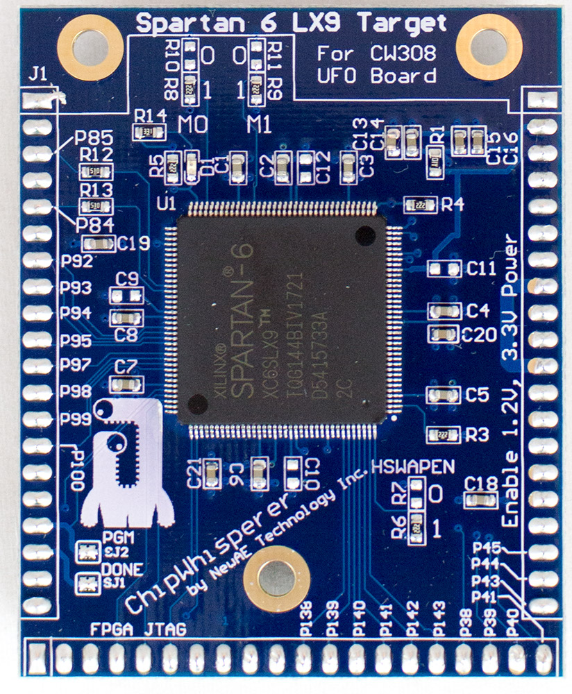
The S6LX9 target is a low-cost FPGA target. It uses the Xilinx Spartan 6 in TQFP package (XC6SLX9-2TQG144C), and can fit an entire AES core. The example project includes the Simple-Serial interface which allows it to function like any of our other example targets.
Specifications
| Feature | Notes/Range |
|---|---|
| Target Device | Spartan 6 LX9 |
| Target Architecture | FPGA |
| Vcc | 1.2V |
| Programming | JTAG |
| Hardware Crypto | Yes |
| Availability | Standalone |
| Status | Released |
| Shunt | 1Ω |
Available from Mouser and the NewAE Store
Usage
The board includes a single red LED (D1) which is connected to the FPGA "DONE" pin. This pin will be HIGH (and the LED on) when the FPGA is NOT programmed. That is to say immediately on power-on, the LED will be on. Once the FPGA is successfully programmed this LED will go out.
The FPGA pins are connected to the various headers on the board. The JTAG header connects to the FPGA JTAG pins. The "Hx" pins, USART, and SPI connect to arbitrary FPGA pins.
'''NB: You MUST enable the 1.2V regulator when using this board. The 1.2V power LED should be ON. This is easily done by toggling the position of the 1.2V LDO switch (to either come from the 3.3V from CW-Lite, or external power depending on your setup). '''
Example Project
The GIT repo includes an example Xilinx ISE project, located at firmware/fpgas/aes/ise/. To use this project:
- Build the bitstream (or see the pre-built one in the repo at cw308t_s6lx9_example.bit)
- Use settings as in the 'Default XMEGA' or 'STM32Fx' targets (i.e., clock jumpers, etc).
- Ensure you have turned on the 1.2V & 3.3V power supplies to the UFO target.
- Program the bitstream into the FPGA using a programming tool such as Xilinx Impact + USB Programmer cable.
- Connect to the ChipWhisperer scope and call
scope.default_setup() - The target supports SimpleSerial v1.0, meaning that it won't ACK. If using
capture_trace(), call as follows:cw.capture_trace(scope, target, text, key, ack=False) - Adjust the trigger offset settings - they should be changed to around \~750, and you can reduce the number of data points to \~128.
The waveform should look something like this:

Known Issues
Note the -02 Revision of the PCB has swapped the markings of the CLKIN/CLKOUT. The correct pinout is:
- CLKIN connects to P84
- CLKOUT connects to P85
The CLKIN pin is a _N clock pin. If you need the _P clock pin, you can use a jumper on the CW308 board to route the clock input into the CLKOUT pin.
Programming
The ChipWhisperer will eventually support programming this target. Until then, you will need an external programmer. This is connected via JTAG to the pin headers:

Options for programmers include:
- Xilinx Platform Cable USB or USB-II (Digikey/Mouser).
- Clone JTAG programmers off AliExpress/E-Bay for low cost (search 'Xilinx JTAG').
- Digilent Inc HS1/HS2/HS3 Cables (NB: you may need separate jumper wires).
To use IMPACT:
- Generate a new project.
- Assign the .bit file to the FPGA (say 'no' to attached SPI flash chips).
- Program.

Schematic
See GIT Repo for PDF of schematic.


Board Layout
See GIT Repo for gerber files.