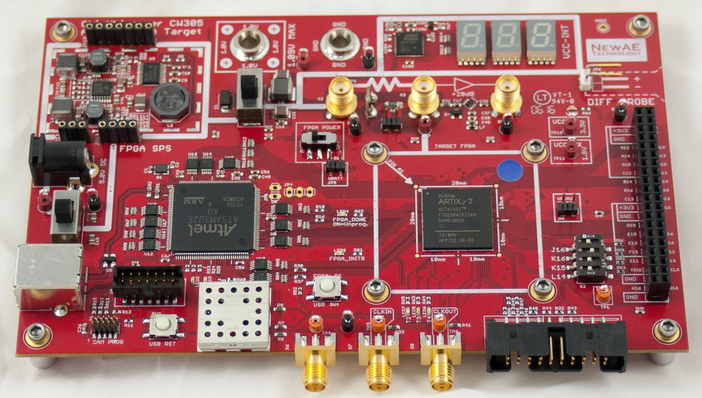
CW305 Artix FPGA Target
The CW305 is a standalone FPGA target board. It features a USB interface to talking to the FPGA, an external PLL for clocking the FPGA, a programming VCC-INT supply, and diode protection for use in fault injection environments. The CW305 board is available in a number of configurations
Like with other ChipWhisperer standalone targets, it requires an external device for side channel power analysis or fault injection and features the standard ChipWhisperer 20-pin/SMA interface.
Specifications
| Feature | Notes/Range |
|---|---|
| Target Device | Xilinx Artix-7 |
| Target Architecture | Xilinx 7 Series |
| Programming | USB, JTAG |
| Hardware Crypto | Yes |
| Availability | Standalone |
| Status | Released |
| Shunt | varies |
USB Control
| Feature | Notes/Range |
|---|---|
| USB | USB 2.0 High Speed |
| VendorID | 0x2B3E |
| ProductID | 0xC305 |
| Interfaces | Vendor |
| WCID (Windows 10 automatic driver installation) | ✔ (firmware >= 1.1) |
- CW305-A35: Available from Mouser
- CW305-A100: Available from Mouser
- CW305-SOCKET: Available from Mouser
Also available in various configurations from the NewAE Store . The NewAE Store is normally updated with available stock, so not all models will be present via the store. The Mouser system will allow backorders so always has all items.
Basic Hardware Overview
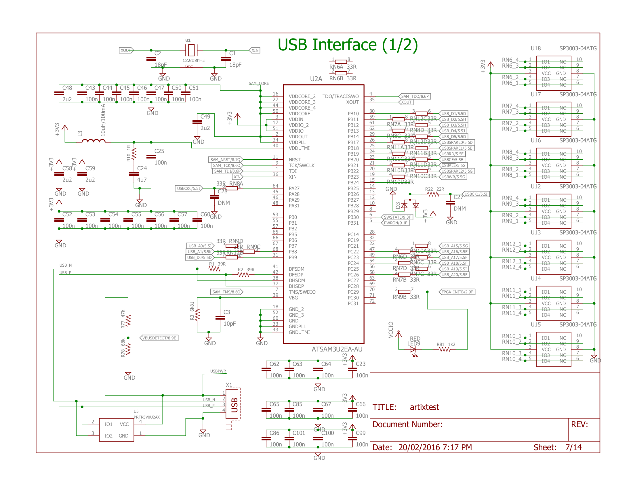
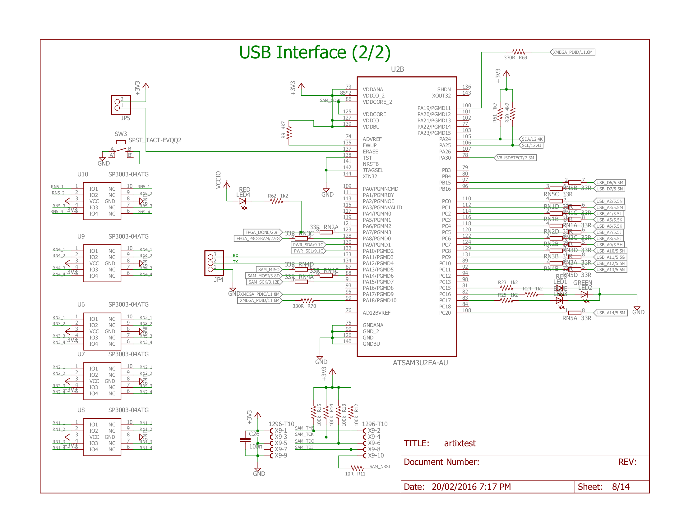
USB Interface
The USB interface for the CW305 implements the higher lever
simpleserial commands, such as simpleserial_read() and simpleserial_write().
For lower level communication, the CW305 allows you to directly
read and write to registers and does not feature the serial read()/write()
like with the SimpleSerial class. For full documentation, see
the CW305 software documentation
To reduce noise in your power measurements, you may want to disable the USB clock while the encryption operation is happening. Again, this can be done via the Python API.
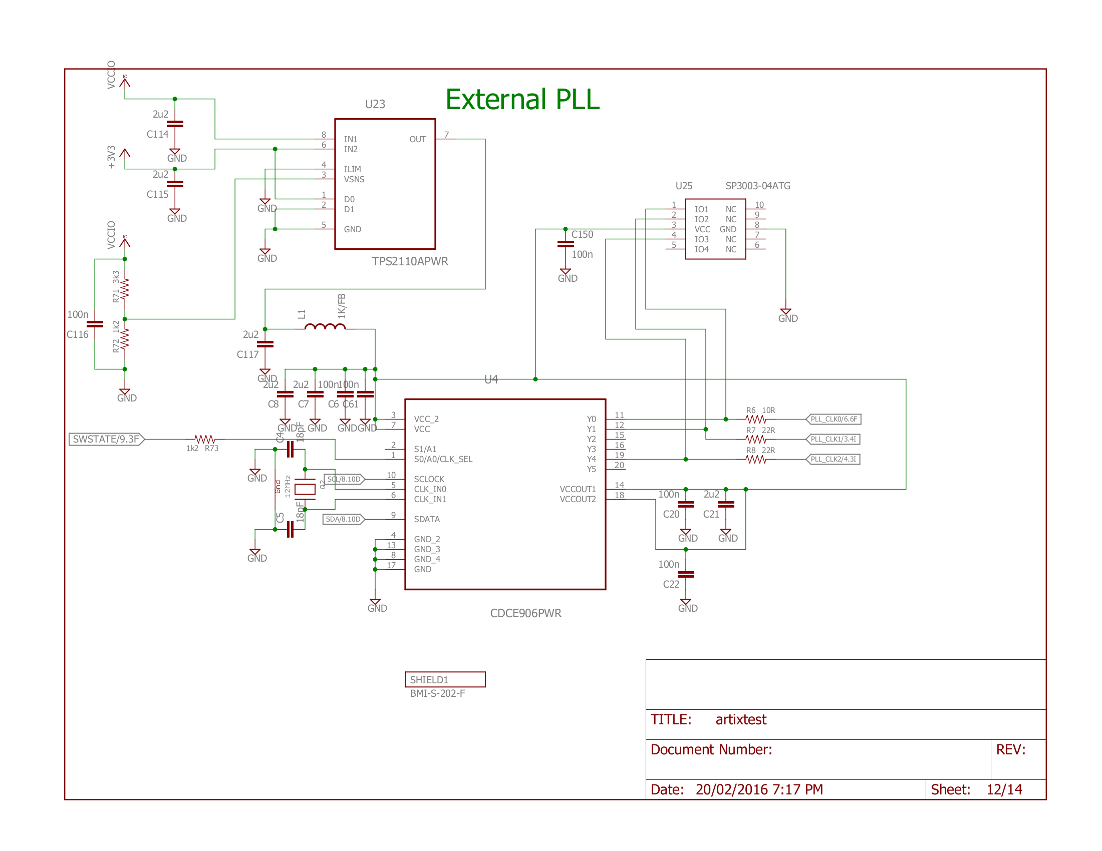
PLL
The CW305 implements a CDCE906 PLL for clocking the FPGA, which can be programmed over USB to output frequencies from roughly 5MHz, to 160MHz. It is capable of outputting 3 channels, with two routed to the FPGA and 1 routed to an output SMA connector. The reference design uses PLL output 1 for the FPGA clock. As the following diagram shows, it has a very flexible architecture:

PLL1 and PLL2 connect to FPGA pins N13 and E12, respectively. The SMA connector X6 can be connected to any of the PLLs, allowing you to get a phase-matched clock on X6 that corresponds perfectly to the clock being fed to the FPGA.
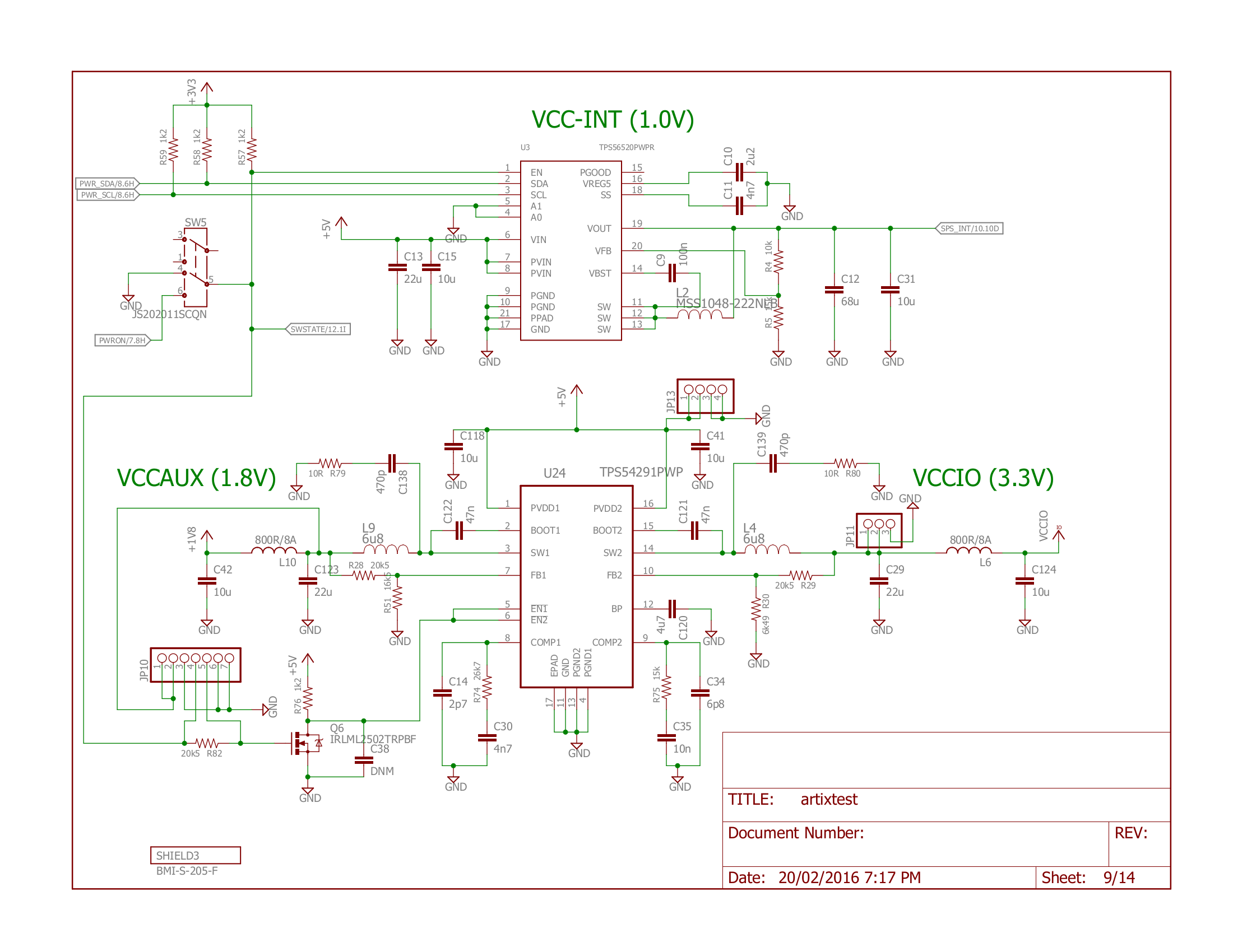
Power Supply
The CW305 board contains three switching regulators. Two are fixed and route to VCC-AUX (1.8V) and VCC-IO (3.3V), while the remaining one can be programmed over USB to output between 0.65V and 1.5V. This is limited in software to a range of 0.8V-1.10V to prevent damage to the FPGA. The VCC-INT regulator is capable of supplying 6A to the FPGA.
Power can be supplied to the CW305 via either the USB-B connector, or via a 5V DC Jack. If you use a large FPGA design, you may exceed the 500mA USB current limit, in which case you must use the DC Jack to supply the board instead. It is suggested that you use a supply that is capable of supplying at least 2A.

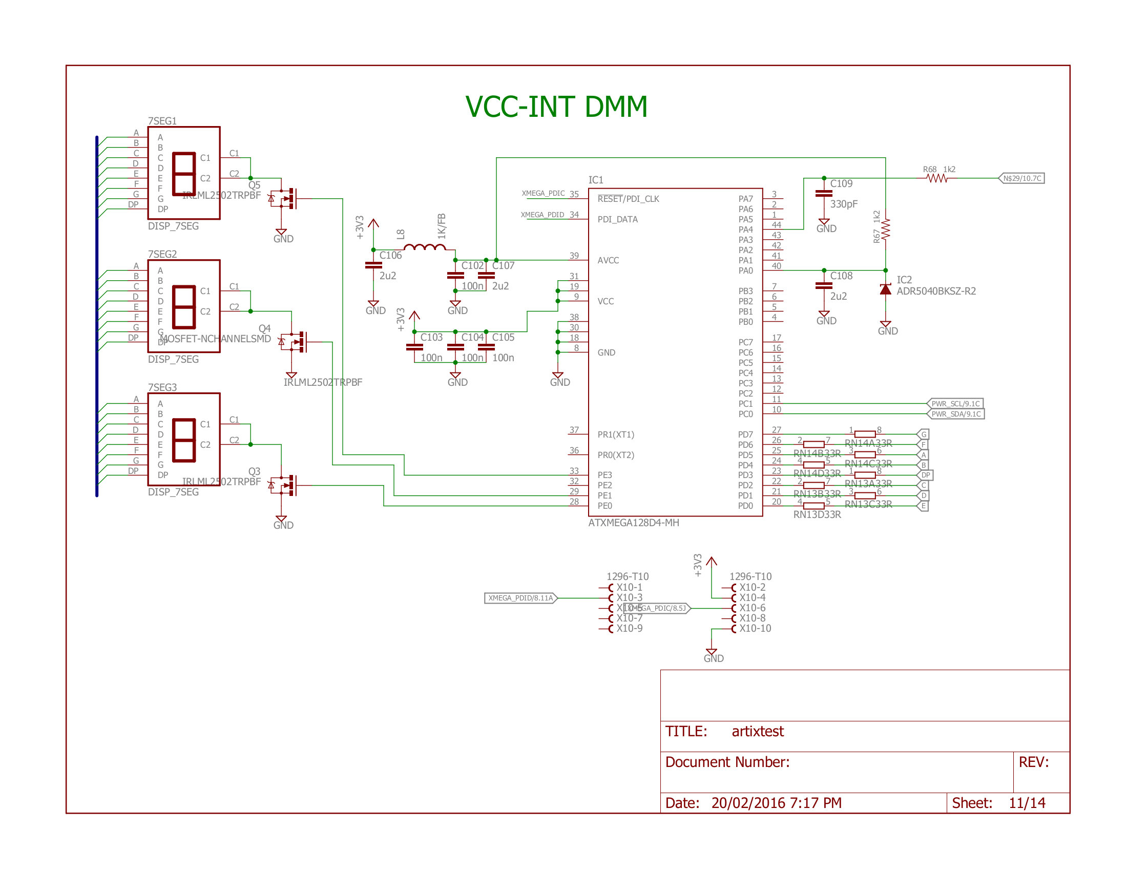
An onboard 3x7 segment display provides an easy visual voltage measurement of VCC-INT so you can confirm settings without needing to attach a multimeter.
The following image shows details of how the power supplies are routed on the CW305 board:

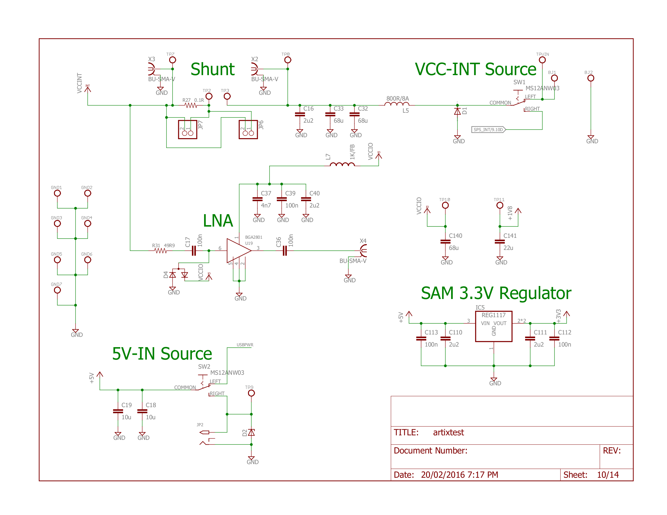
Shunt Measurement
A resistive shunt is located between the VCC-INT supply and the FPGA. SMA connectors provide measurement access to both the high (X2) and low (X3) sides of the shunt, as well as a 20dB low noise amplified low side signal (X4). The shunt resistor can also be measured across via two 0.1" differential probe headers, one (JP7) directly next to the shunt resistor and one (JP6) on the top right of the PCB. JP6 is designed to be used with the CW501 Differential Probe
The shunt resistor can be bypassed by shorting JP7.
The following image shows the area on the PCB around the shunt resistor:

Schematically, this is shown below. NOTE: the schematic flows in the "opposite" direction of the PCB. In the PCB power flows left to right, in the schematic it flows right to left.

In addition, two test points are provided on each side that are suitable for use with an oscilloscope probe. It is strongly recommended to use a SMA to BNC cable (such as Cinch Connectivity P/N 415-0028-024 available from Digikey) to view the power measurement instead of these test points, as the SNR of the oscilloscope probe will typically be considerably worse than via the SMA connector.
Depending on your use case, you may want to experiment with different values of shunt resistor. For example, the default shunt resistor may cause too much voltage drop for larger designs. Examples of shunt resistors can be seen in the table below:
| Value | Manufacturer | Part Number |
|---|---|---|
| 500mΩ | Stackpole | CSR1206FKR500 |
| 250mΩ | Stackpole | CSR2016FKR250 |
| 100mΩ | Samsung | RUW3216FR100CS |
| 50mΩ | Vishay | WSLP1206R0500FEA |
Fault Injection
The CW305 is designed to facilitate all forms of fault injection. Resistive and diode protection prevents transients on the VCC-IO of the FPGA from affecting the USB interface chip. The USB chip itself provides high-speed FPGA reconfiguration to simplify repetitive fault attacks where you need to reconfigure the FPGA. The USB interface can also monitor the INITB pin of the FPGA, which can be used with the continuous CRC verification feature to determine when reconfiguration is required.
Crowbar faults can be injected on the low side of the shunt resistor using SMA connector X3. The PCB also features mounting holes and alignment features for use with an X-Y table (suitable for both EM fault injection and an H-Field probe).
Note that the VCC-INT banana plugs are not suitable voltage glitching points as filtering is present after them.
If using an external fault amplifier, connect again to X3, and remove the jumper next to the shunt resistor as described in Jumper
Advanced Hardware Overview
Reprogramming the USB Interface (SAM3U)
Like with other ChipWhisperer hardware with a USB interface, the onboard SAM3U microcontroller providing the interface can be reprogrammed. The bootloader can be entered and new firmware can be uploaded using the same interface as the ChipWhisperer Capture hardware: https://chipwhisperer.readthedocs.io/en/latest/firmware.html.
There is also a Cortex Debug Connector located near the USB-B connector that can be used to program and debug the SAM3U. See details at end of page for SAM3U firmware.
Power Supply/Measurement
Powering VCC-INT with an External Supply
You may want to use your fancy, super low noise external power supply instead of the onboard switching power supply for VCC-INT. This can be done by feeding power into the two banana jacks on the board. Be very careful to ensure you do not exceed 1.10V on this input, as feeding in too high of a voltage can damage the FPGA.

The choice of internal/external supply is selected with a switch located right beside the positive banana jack input. There are large capacitors and a ferrite bead on this input, so it is not suitable for inserting voltage glitches.
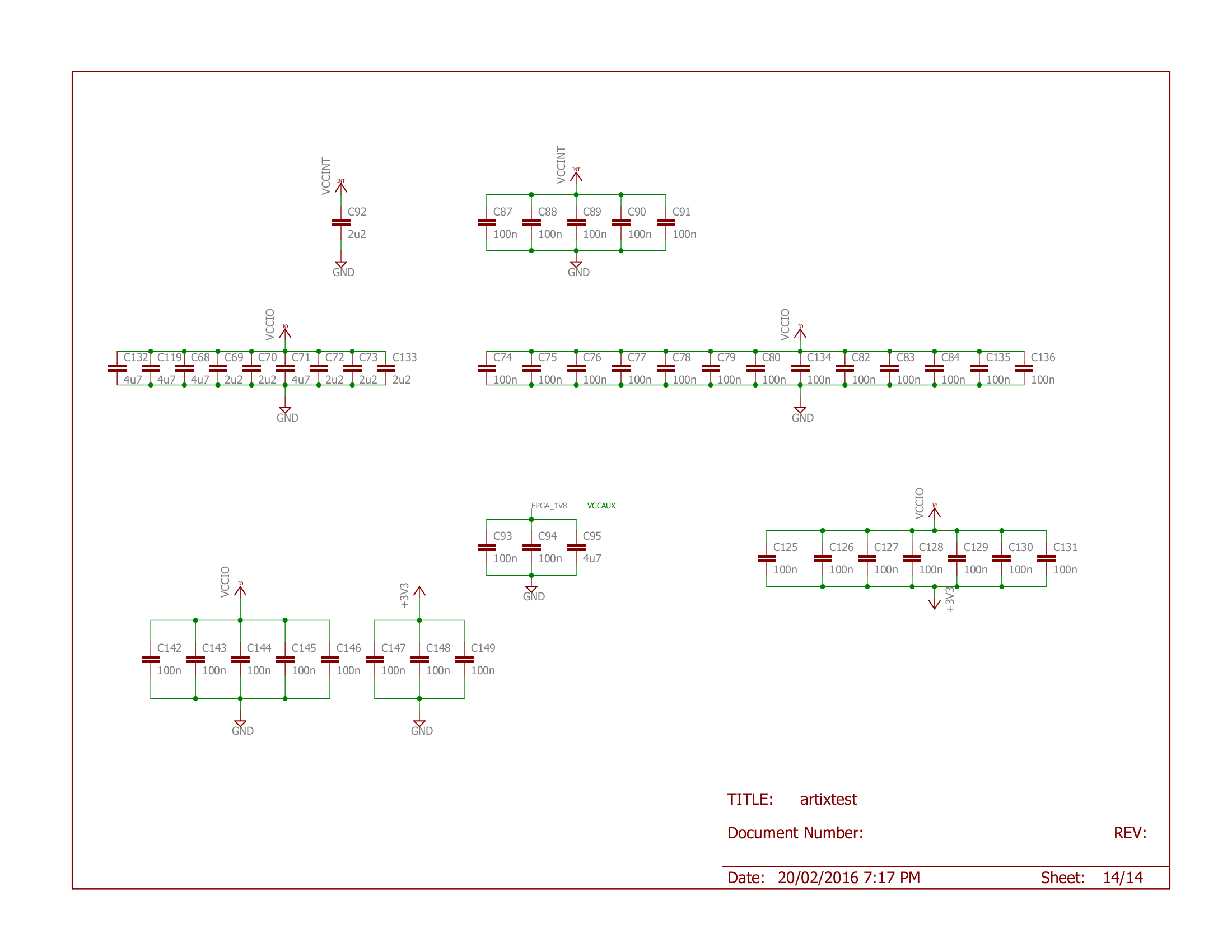
VCC-INT Decoupling Capacitors
Optional decoupling capacitors can be mounted on the low side of the VCC-INT shunt. They are located on the bottom of the board and are typically not mounted when using the shunt resistor to measure power waveforms.
The optional decoupling capacitors for the VCC-INT rail are shown on the underside of the PCB here:

VCC-AUX Shunt Resistor
The VCC-INT shunt is the primary power measurement point, as it provides power measurement for both designs inside the FPGA, as well as the logic for decrypting bitstreams (as reported at https://eprint.iacr.org/2016/249.pdf).
There may be additional information in the VCC-AUX power supply, such as JTAG state transitions. There is a secondary shunt position (by default with no shunt mounted) for exploration of the VCC-AUX power supply. This can be seen in the schematic here:

The shunt is located on the rear side of the PCB, as shown here:

If using this shunt, you must remove resistor R26 (which has a metal slug 0-ohm resistor mounted) and replace with an appropriately sized 0805 resistor (suggested: 1 ohm). You must also remove capacitor C98, C95, C97, C94, and C93. They can be seen in the above photo.
Low Noise Power Supply
Optional low-noise linear power supplies are available, which fit into the connectors around the switch-mode power supply. They have less power handling capabilities than the on-board switch-mode supplies, but have reduced noise that ends up injected into the PCB (and thus on the power traces).
These power supplies are only used for VCC-IO and VCC-AUX. Like the on-board supplies they will be disabled when the power to the FPGA is switched off using the target power switch.
If you wish to have the lowest-noise power source, you must mount the VCC-IO and VCC-AUX low-noise supplies, and also use an external supply for the VCC-INT supply.
Jumper
In some circumstances you may wish to entirely remove the shunt resistor. This is typically the case when performing fault insertion, where the large "filter" capacitors present on the high side of the shunt resistor will drastically reduce the slew rate of your fault amplifier.
Alternatively, you may wish to use a current transformer or similar current probe which requires a method of inserting a sensor into the VCC-INT path.
For these uses test point TP2 and TP3 have gold-plated "nails" soldered into them, and a wire bridge soldered between the test points. This wire bridge can be removed by either cutting (with wire cutters) or desoldering. The gold-plated nails provide a mechanically strong base which allows you to perform this operation without risking damage to the CW305 PCB.
If using a current probe, you can either (1) solder a wire between TP2 and TP3, or (2) use two SMA connectors to route the power between X2 and X3. Clamp your current probe onto the bare wire used to route the signal between these (you'll need a custom cable without the shield most likely).
The gold-plated nails that require soldering are used instead of a switch or jumper to reduce the resistance in the measurement path. Typical switches provide too high of a contact resistance for the potential current draw of a large design in the FPGA, which would reduce the SNR at the measurement point.
Power Cycling the Board
The CW305 can be power cycled via SW5:

When in the "OFF" mode the VCC-INT, VCC-IO, and VCC-AUX supplies are turned off. In addition the communications interfaces are all disabled to avoid back-powering the FPGA via the IO pins. If you have external connections (such as driving a clock from the ChipWhisperer) you need to ensure they are also disabled when the power is turned off.
I/O and LEDs
GPIO Header
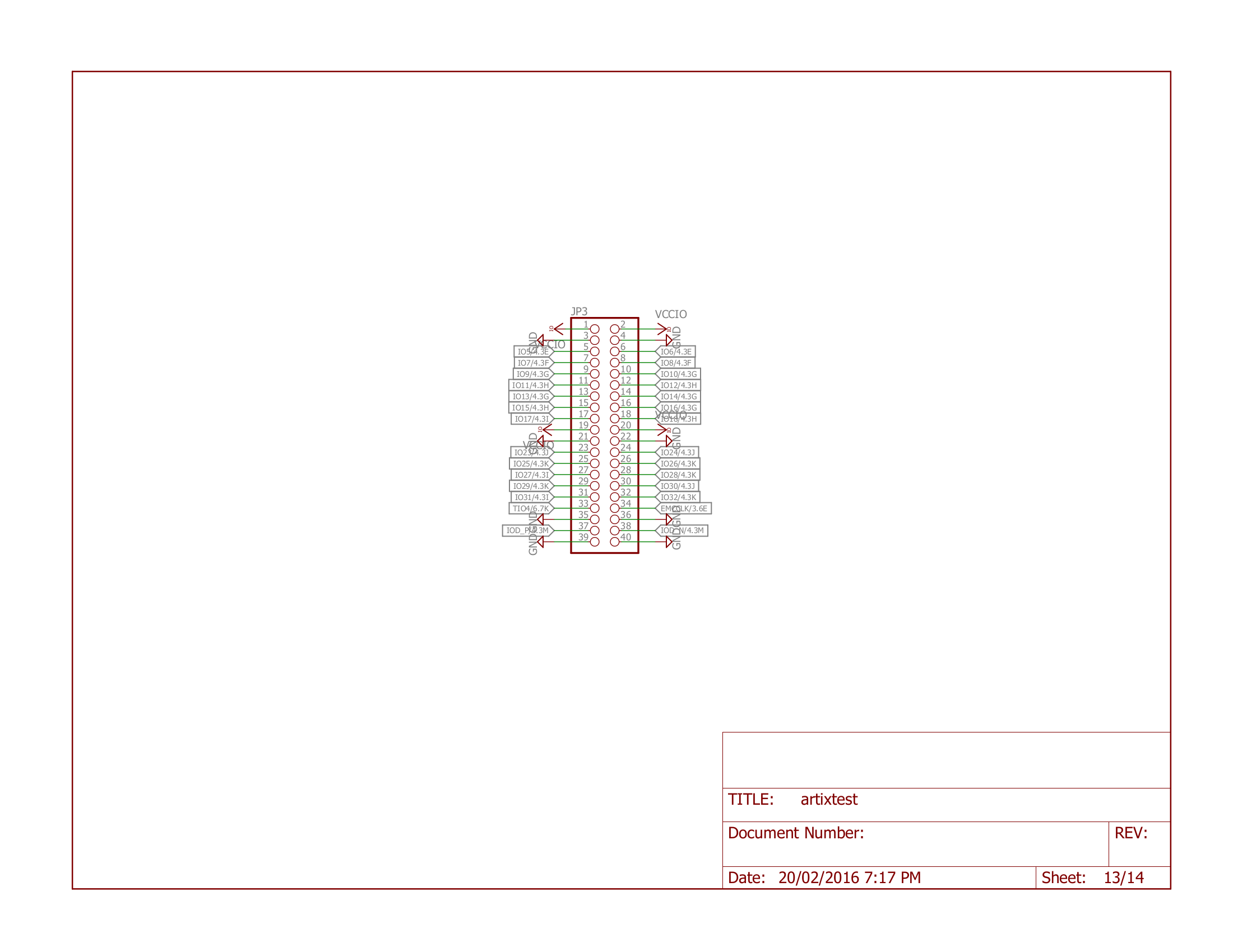
A 40-pin header is mounted at JP3. This female header also comes with a dual-sided male 40-pin header which ships which each PCB, allowing you to use either gender of connectors with this header.
The pinout of the header is marked on the PCB. All pins are routed to 3.3V VCC-IO banks on the Artix 7 FPGA. The layout of the header is such that the following can directly be plugged into the board:
- Digilent Inc PMOD Devices
- NewAE OpenADC Module
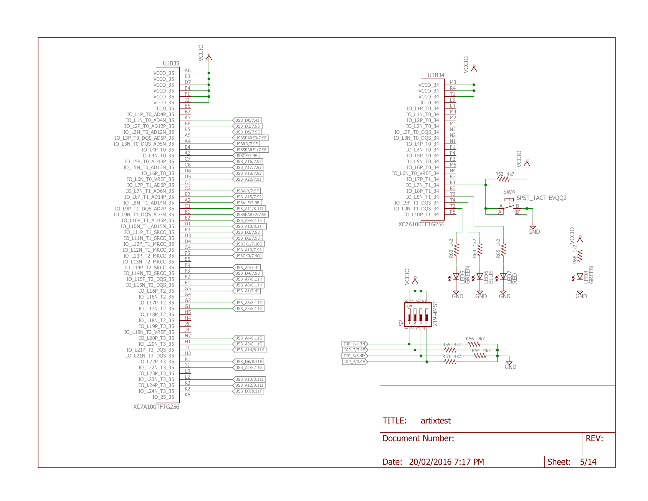
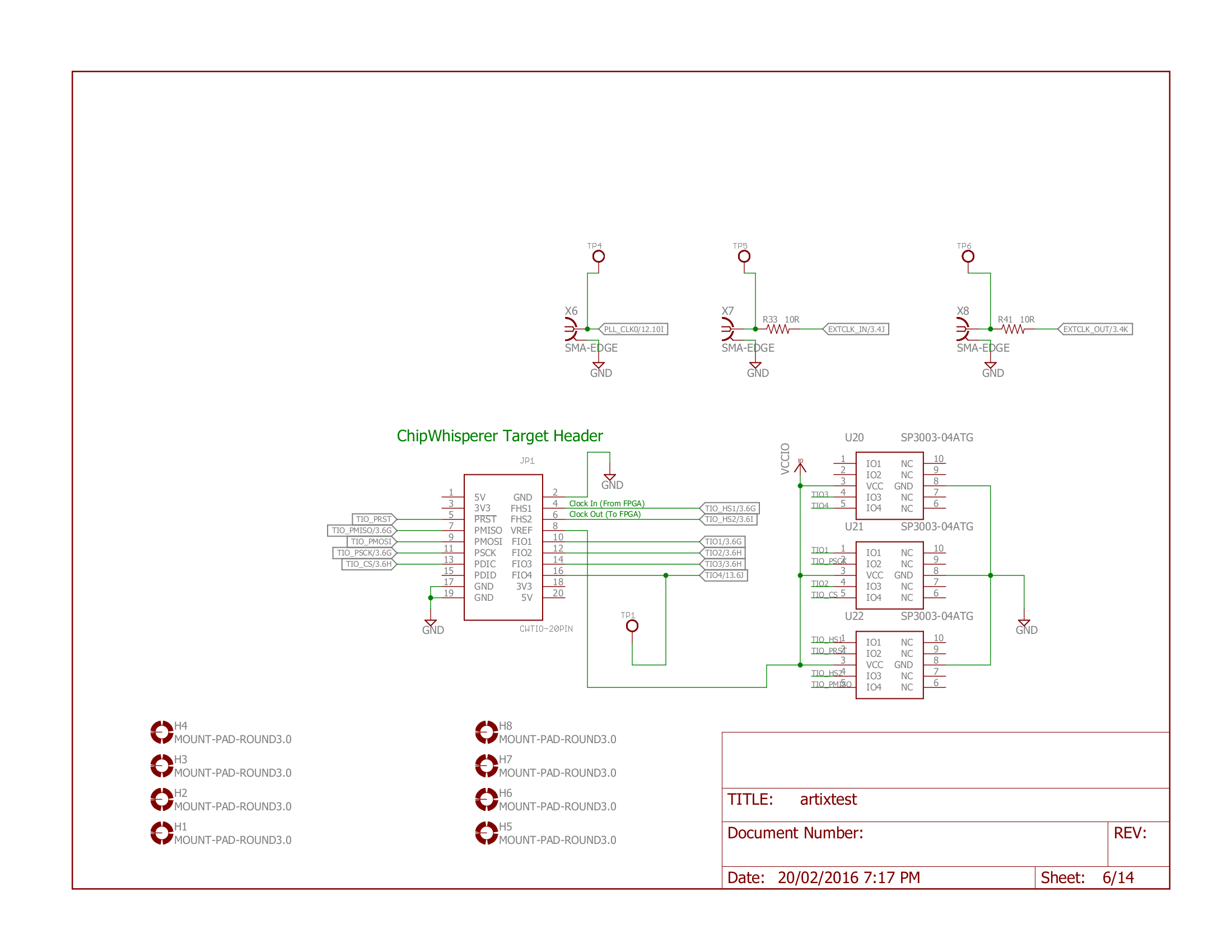
ChipWhisperer 20-pin Connector
The bottom right side of the PCB contains a 20-pin connector that follows the standard ChipWhisperer pinout. This connector has ESD diodes present on the PCB to protect both the FPGA from external transients, and from glitches inserted into the FPGA from exiting the board and damaging external test gear.
Clock SMA Connectors
Three additional SMA connectors are provided that output directly from a PLL channel (X6), allow you to feed a clock input into the FPGA (X7), or output a clock signal from the FPGA (X8).
Switches
Two user switches are provided: one push-button and one 4-item DIP switch.
The push-button (SW4) routes to FPGA pin R1.
The dip-switch (S2) routes to FPGA pins J16, K16, K15, and L14. With the reference FPGA design, the dip switch has the following uses:
| J16 | Input Clock Source |
|---|---|
| 1 | ChipWhisperer HS-IO |
| 0 (Default) | PLL1 |
| K16 | ChipWhisperer HS-Out |
|---|---|
| 1 (Default) | Enabled (clock) |
| 0 | Disabled |
See the example design documentation for more details.
Programming the FPGA
In addition to programming the FPGA over the USB interface, the CW305 can additionally be programmed over JTAG from Xilinx Vivado software. With both of these methods, the CW305 must be reconfigured every time the device is power cycled.
There is also an on-board SPI flash chip which can be used to store a bitstream. See more details of the SPI chip programming below.
These different modes are selected using S1 on the back of the board:

The setting of the mode switches must be set as in the following table for the desired configuration mode:
| M0 | M1 | M2 | Configuration Mode |
|---|---|---|---|
| 1 | 0 | 0 | SPI Flash |
| 1 | 0 | 1 | JTAG |
| 1 | 1 | 1 | USB (Default) |
On-Board SPI Memory
The on-board SPI memory chip can be used for your own program storage (when implementing soft-core processors), or can be used for a FPGA configuration bitstream if the mode switches are set as above.
Details of SPI FLASH memory & FPGA usage is seen in XAPP586
Part Numbers
Three part numbers have been used during the production runs (as devices go EOL the part numbers change typically):
| Part Number | Vivado | ISE Impact | Dates | Notes |
|---|---|---|---|---|
| S25FL132K0XMFI04 | ? | Yes | Before 2018 | Part is Obsolete |
| AT25SF321 | No | ? | 2018 - 2021 | May have used AT25SF321A. Both parts now EOL. |
| MX25L3233FMI1-08 | Yes | ? | 2021 - | Boards produced late 2021 onward. Tested in Vivado. |
Some of the SPI chips are not directly supported as a programmable chip from the Xilinx design tools, meaning you cannot use the "Attached Serial Flash" option for those parts from ISE or Vivado. You can use the built-in USB programmer instead for those flash chips, as described next.
Note that ISE Impact supported using a XIL_IMPACT_SKIPIDCODECHECK=1 environment variable, which caused Impact to work with any compatible memory even if the
IDCode was not exactly the same. ISE Impact supports only the Artix A100, it does not support the Artix A35 FPGA. Thus even if you install ISE 14.7 (no longer trivial), it may not support your CW305 board.
Vivado does not support this override option, and requires the IDCode to match exactly. Note that if Vivado finds an attached SPI flash memory with an
IDCode that does not exactly match the expected one, it will report the IDCode as being 0, 0, 0 (even if the IDCode was correctly read as non-zero). Due to
the difficulty in debugging this, we typically recommend using the USB programming described next instead.
Programming over USB
Recently, the ChipWhisperer software integrated support for programming the SPI flash directly. This requires you to load a small "shim" bitstream into the FPGA, which connects the SPI flash pins to the SAM3U.
This means during SPI programming your FPGA design will be cleared. You can reload your FPGA design of course afterwards, but if you are using a soft-core type system you should program the SPI flash first, then load your FPGA bitstream (which will clear out the SPI-flash bitstream).
SPI API documentation for this can be found on our ReadTheDocs page
Note you'll need to adjust the mode switches back and forth for this to work - the switches need to be set to allow USB programming for the shim to work, then can be switched back to load from the on-board SPI flash.
Generating SPI Flash files from Vivado
To generate the .mcs or .bin files inside of Vivado, use the write_cfgmem command. You'll need to change directory first for this to work. An example run is shown below:
cd C:/dev/chipwhisperer/hardware/victims/cw305_artixtarget/fpga/vivado_examples/aes128_verilog/aes128_verilog.runs/impl_35t
write_cfgmem -format mcs -interface SPIx1 -size 32 -loadbit "up 0x0 cw305_top.bit" -file cw305_a35_aes.mcs
write_cfgmem -format bin -interface SPIx1 -size 32 -loadbit "up 0x0 cw305_top.bit" -file cw305_a35_aes.bin
The .mcs file can be used by Vivado, and the .bin can be used by Vivado or the ChipWhisperer programming tool described above.
When using the SPI on-board chip to boot me sure you adjusted the mode switches. You can toggle the FPGA power with switch SW5 to force it to reload after changing the mode switches, or toggle the PGM pin via software.
SAM3U Firmware
The firmware for the SAM3U is open-source and can be modified as you wish. See hardware/victims/cw305_artixtarget/fw/sam3u/CW305_SAM3U_FW for the firmware in the ChipWhisperer repository.
Currently, you build it with:
cd src
make clean
make
This will generate a file called ChipWhisperer-CW305-SAM3U1C.bin you can program in, or ChipWhisperer-CW305-SAM3U1C.bin you can load in something like
Ozone if you have a debugger attached.
Re-Programming SAM3U via Python
import chipwhisperer as cw

# or CW305 target object
programmer = cw.SAMFWLoader(scope=fpga)
# WARNING: this will erase the firmware on the device
# and make it unusable until reprogrammed.
programmer.enter_bootloader(really_enter=True)

#Wait a moment for device to re-enumerate as USB-serial
programmer = cw.SAMFWLoader(scope=None)
programmer.program("com4", r"..\..\hardware\victims\cw305_artixtarget\fw\sam3u\CW305_SAM3U_FW\src\ChipWhisperer-CW305-SAM3U1C.bin")

#Power cycle CW305 using switch
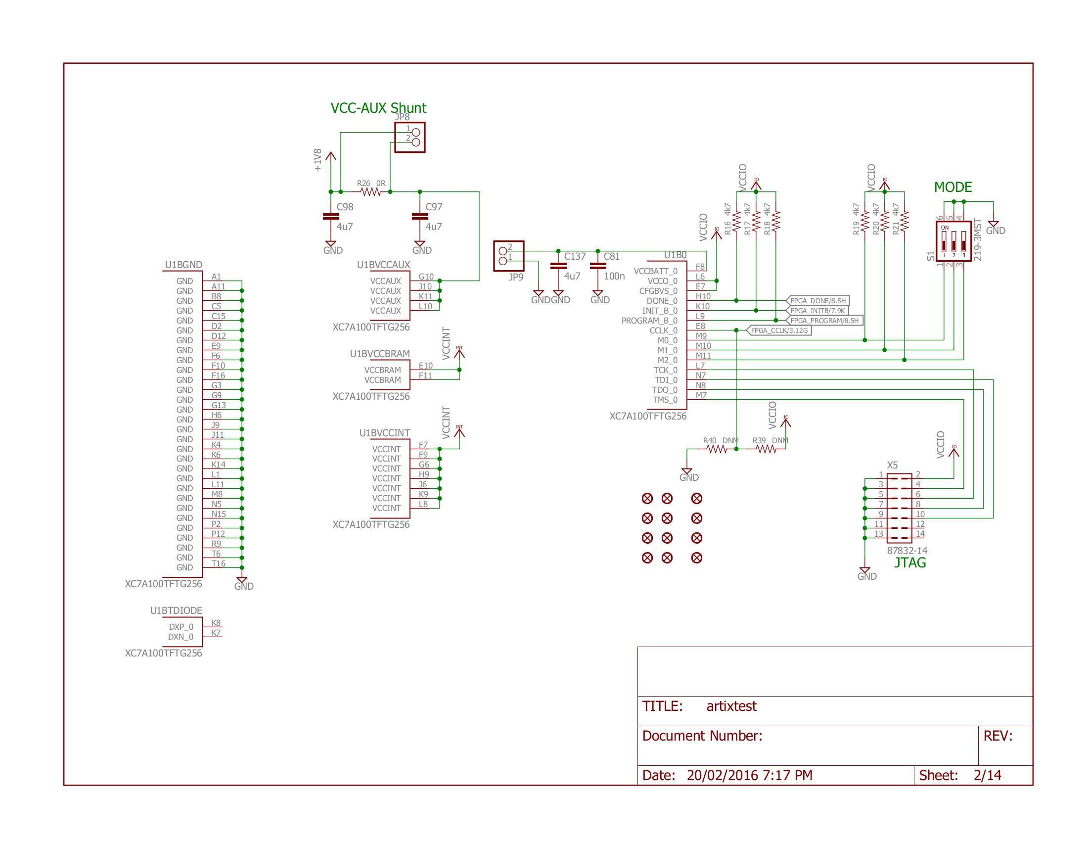
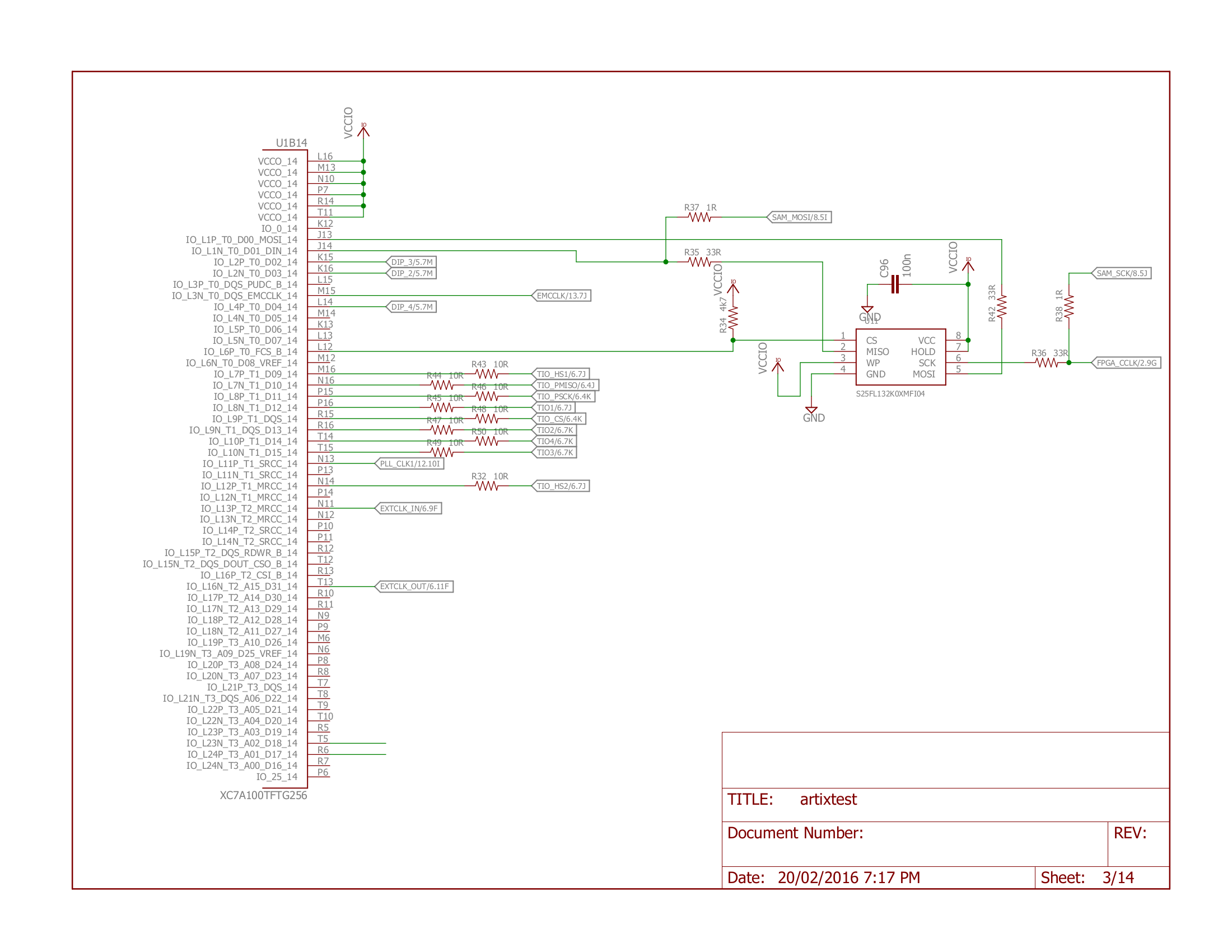
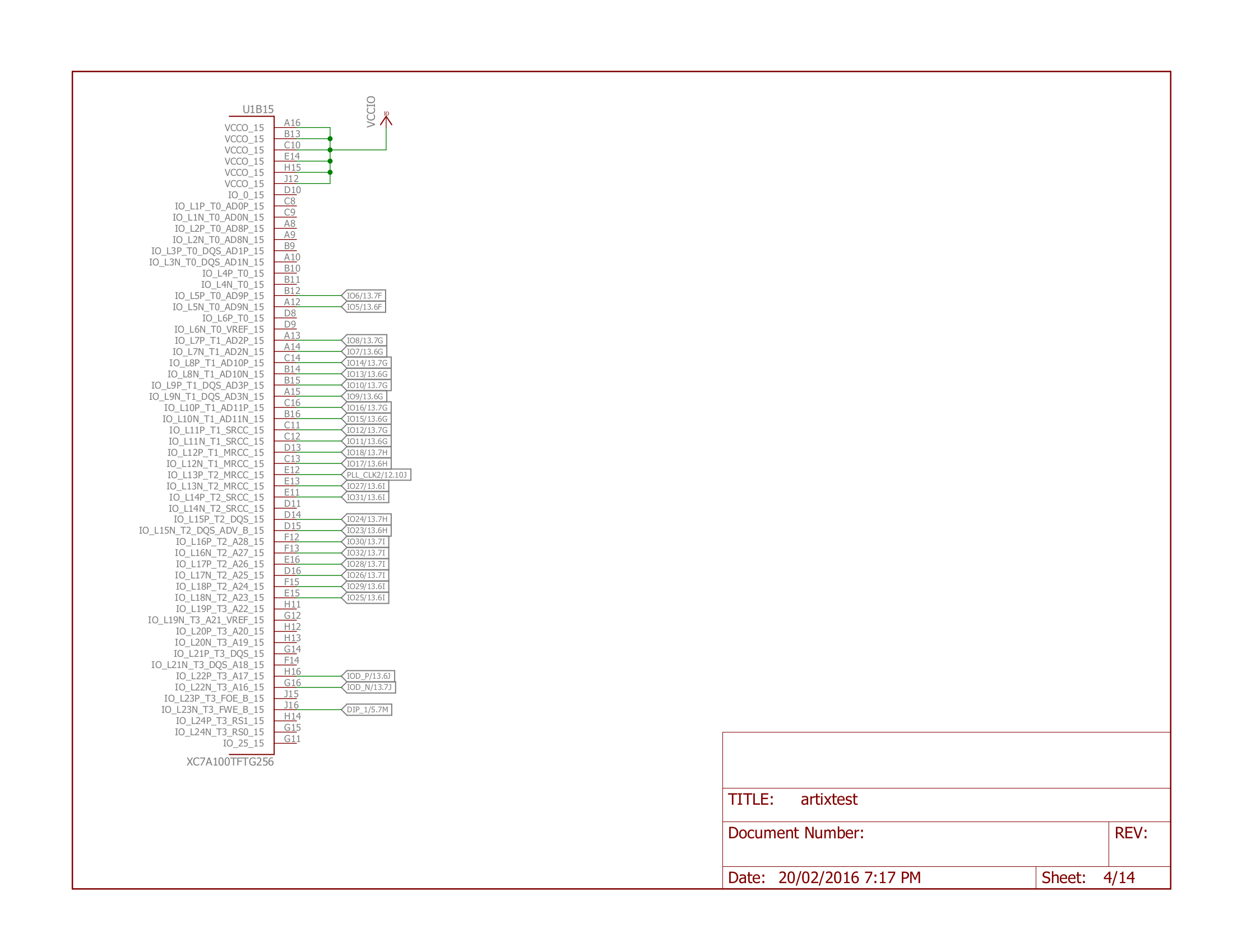
Schematic
You can get the full schematic in PDF format from the git repo. See below for individual pages.